Complimenting our September 2019 International Patent Calendar (which focused mostly on methods of anodizing aluminum), this month’s collection of patents focuses on special applications of anodized aluminum surfaces. The uniqueness of anodized aluminum oxide coatings in terms of their chemical, physical, and mechanical properties has resulted in many innovations in various industrial and scientific fields, especially in electronic devices and unique applications in the automotive and aerospace fields. The scope of innovation in specialized applications of anodized aluminum coatings is indeed international as the selected inventions presented here demonstrate.
Of the 37 inventions selected below, the majority focus on electronic innovations that depend on special properties of anodized aluminum surfaces: capacitors (one of which is used in pacemakers), housings, printed circuit laminates, semiconductors, electrode structures, and sensors.
In addition, there are nine patents on antireflective (AR) anodized aluminum surfaces for display devices. These AR patents have a biomimetic connection and are sometimes called “moth-eye” structures that form arrays of protuberances smaller than the wavelength of light incident upon them, thus greatly reducing the light reflected by the surface. Such structures are found on the eyes of some species of moths where the light reduction in reflectance increases visual sensitivity. Display devices used in televisions, cell phones, camera lenses, etc. adopt AR techniques to increase light transmission and reduce light reflection using specially prepared anodized aluminum surfaces with an inverted “moth-eye” structure attached to a mold or “stamper” that imparts the desired nanoimprinted characteristics on an AR film.
In the automotive field, some of the patents presented here are mostly involved in applications requiring the high hardness of anodized coatings for superior wear and scratch resistance. In the aerospace field, the applications of anodized coatings require that they be multifunctional to meet requirements of corrosion resistance and suitability for painting and adhesive bonding, especially on the high strength aluminum alloys used. Three of the patents selected deal with the coating requirements needed for efficient lithographic printing, where the anodizing baths require special chemistries and anodizing process parameters.
Altogether, aluminum anodized surfaces serve multiple functions, with the largest among these corrosion protection and cosmetic finishes, which the building and construction and transportation industries heavily rely on. However, several important industries — the electronics industry, for one — depend on specialized anodized aluminum surfaces that may represent a fraction of the anodized aluminum surface area produced overall in order to meet the stringent requirements expected of their products. Some of these inventions presented below demonstrate the wide range of possibilities that specialized anodized aluminum offers. Future Light Metal Age patent reviews will survey many more anodized aluminum inventions in processing and applications that solve some of the most challenging industrial problems.
– Joseph C. Benedyk, Editor
US9512510 — HIGH-STRENGTH ALUMINUM ALLOY AND PROCESS FOR PRODUCING SAME — UACJ Corporation (Japan) — The present invention relates to a high-strength aluminum alloy material that can be used at portions where both strength characteristics and appearance characteristics are considered to be important. A high-strength aluminum alloy material having a chemical composition which includes Zn: more than 7.2% (mass %, the same applies hereafter) and 8.7% or less, Mg: 1.3% or more and 2.1% or less, Cu: 0.01% or more and 0.10% or less, Zr: 0.01% or more and 0.10% or less, Cr: less than 0.02%, Fe: 0.30% or less, Si: 0.30% or less, Mn: less than 0.05%, Ti: 0.001% or more and 0.05% or less, the balance being Al and unavoidable impurities, is provided. It has a proof stress of 350 MPa or more, and a metallographic structure formed of a recrystallized structure, and L* and b* values, as defined in JIS Z8729 (ISO 7724-1), are 85 or more and 95 or less and 0 or more and 0.8 or less, respectively, as measured after anodization using a sulfuric acid bath. Since an aluminum alloy having L* and b* values falling within the above-described ranges exhibits a silver color when visually observed, the above-described high-strength aluminum alloy material is a material that excels in design properties after anodization.

US9508461 — POLYMERIC OVERCOATED ANODIZED WIRE — Ford Global Technologies, LLC (USA) — An insulated electric conductor and method for making such a conductor are disclosed. The conductor comprises a copper core, a layer of aluminum formed over the copper core, an aluminum oxide dielectric layer formed over the layer of aluminum, and a thin polymeric layer formed over the aluminum oxide dielectric layer. The thin polymeric layer is preferably between about 30 microns (0.001”) and about 500 microns (0.02”) and is more preferably between about 45 microns (0.0015”) and about 250 microns (0.01”). The polymeric layer may be any polymeric material selected from the group consisting of acrylic resins, epoxy resins, polyurethane resins, and silicone resins. Other polymeric materials may be used. The polymeric layer may be formed by a variety of methods including, but not limited to, spraying, brushing, dipping, and powder coating. The insulated electric conductor of the disclosed invention offers many advantages in application and operation and may find superior utility in high power electrical motors, high voltage traction battery subsystems, generators, alternators, and in hybrid vehicles and operating systems for such vehicles.

US9476137 — METAL OXIDE FILM, LAMINATE, METAL MEMBER AND PROCESS FOR PRODUCING THE SAME — Tohoku University and Mitsubishi Chemical Corporation (Japan) — This invention relates to a metal oxide film, a laminate, a metal member, and their manufacturing methods and, in particular, relates to a metal oxide film, a laminate, and a metal member suitable for use in a manufacturing apparatus used in the manufacturing process of an electronic device such as a semiconductor or a flat panel display, and to methods of manufacturing them. A metal oxide film suitable for protection of metals, composed mainly of aluminum. A metal oxide film includes a film of an oxide of a metal composed mainly of aluminum, having a thickness of 10 nm or greater, and exhibiting a moisture release rate from the film of 118 molecules/cm2 or less. Further, there is provided a process for producing a metal oxide film, wherein a metal composed mainly of aluminum is subjected to anodic oxidation in a chemical solution of 4 to 10 pH value to obtain a metal oxide film.
US9475954 — HIGH-HARDNESS CLEAR COATING MATERIAL — Hyundai Motor Company and Kia Motors Corporation (Korea) — The present invention relates to a high-hardness clear coating material, and in particular, to a high-hardness clear coating material capable of improving the hardness and gloss of aluminum. This is a technology for forming an anodizing layer (2) having high hardness through an anodizing treatment and forming a clear corrosion resistant coating layer (3) to improve gloss and corrosion resistance. The high-hardness clear coating material capable of improving hardness and corrosion resistance of an anodized aluminum material surface includes, in % by weight, 10 to 20% of a melamine curing agent, 10 to 15% of silica, 1 to 5% of a phenol resin, and a remainder of an acrylic resin and other unavoidable impurities.
US9458549 — METHOD FOR MANUFACTURING OF AN OBJECT HAVING PHOSPHORESCENT PROPERTIES — Alusera AB (Sweden) — Objects with surfaces having luminous afterglow (phosphorescent) properties are useful as indicators of, for instance, emergency equipment where they can be used to indicate escape routes and location of critical equipment in darkness, such as in the event of a power failure in public buildings or during an emergency situation on a ship or an aircraft. Introduction of phosphorescent properties can also be used for gadgets, toys etc. The invention concerns a method for manufacturing of an object having phosphorescent properties, comprising the steps of providing an object having a surface made from aluminum or from an aluminum-based alloy and forming a layer of porous aluminum (hydr)oxide at said surface. The invention is characterized in that the method comprises the step of contacting the layer of porous aluminum (hydr)oxide with one or several solutions containing metal dopant ions such as to allow the metal dopant ions to bind to the layer of porous aluminum (hydr)oxide, wherein at least one of said solutions contains ions of at least one element selected from a first group consisting of calcium (Ca), magnesium (Mg), strontium (Sr) and barium (Ba), and wherein at least one of said solutions contains ions of europium (Eu). The invention also concerns an object obtainable by the above method.
US9457493 — METHOD FOR PRODUCING CYLINDRICAL NANOIMPRINTING MOLD AND METHOD FOR PRODUCING NANOIMPRINTING REPRODUCTION MOLD — Mitsubishi Rayon Co., Ltd. (Japan) — Provided is a method for producing a cylindrical nanoimprinting mold such that the outer peripheral surface of a cylindrical aluminum substrate is uniformly polished, and it is possible to effectively take advantage of the outer peripheral surface. The method forms an oxide film at the outer peripheral surface (14) of an aluminum substrate (10) after polishing the entire outer peripheral surface (14) of the cylindrical aluminum substrate (10) by means of a polishing body (26), wherein the polishing body (26) is moved in the axial direction to polish in a manner such that at least a portion of the polishing body (26) is protruding beyond the first end (10a) side and second end (10b) side of the aluminum substrate (10), and the portion of the polishing body (26) protruding beyond the aluminum substrate (10) is disposed on and supported by a cylindrical first support member (18); and second support member (20). The concave-convex nano-scale microstructure so produced exhibits a structure-derived function such as an antireflection function referred to as a moth-eye effect or a water repellant function referred to as a lotus effect. Therefore, the industrial use of this microstructure (improvement in light extraction efficiency of organic EL elements, antireflection of image display apparatuses, improvement in image clarity of image display apparatuses, water repellant materials for various members, or the like) is actively made.
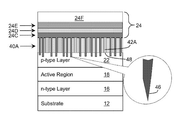
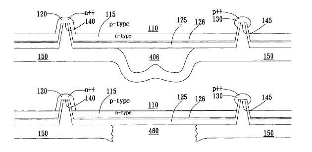
US9425353 — HETEROSTRUCTURE INCLUDING ANODIC ALUMINUM OXIDE LAYER — Sensor Electronic Technology, Inc. (USA) — A semiconductor structure including an anodic aluminum oxide layer is described. The anodic aluminum oxide layer can be located between a semiconductor layer and another layer of material. The anodic aluminum oxide layer can include a plurality of pores extending to an adjacent surface of the semiconductor layer. The layer of material can penetrate at least some of the plurality of pores and directly contact the semiconductor layer. In an illustrative embodiment, the layer of material is a conductive material and the anodic aluminum oxide is located at a p-type contact.
US9412652 — AIR GAP FORMING TECHNIQUES BASED ON ANODIC ALUMINA FOR INTERCONNECT STRUCTURES — Taiwan Semiconductor Manufacturing Co., Ltd. (Taiwan) — As dimensions and feature sizes of semiconductor integrated circuits (ICs) are scaled down, the density of the elements forming the ICs is increased and the spacing between elements is reduced. As the distance between any two adjacent conductive features decreases, the resulting capacitance increases, which will increase power consumption and time delay. To reduce parasitic capacitance and correspondingly improve device performance, IC designers utilize low-k dielectrics. One kind of low-k material is produced by creating large voids or pores in a dielectric, e.g., in anodized aluminum (Al). Thus, an Al layer is formed over a semiconductor substrate. A selective portion of the Al layer is removed to form openings. The Al layer is anodized to obtain an alumina dielectric layer with a plurality of pores. The openings are filled with a conductive interconnect material. The pores are widened to form air gaps and a top etch stop layer is formed over the alumina dielectric layer.
US9405043 — MOLD AND PROCESS FOR PRODUCTION OF MOLD — Sharp Kabushiki Kaisha (Japan) — A mold manufacturing method of the present invention is a method for manufacturing a mold which has an inverted moth-eye structure over its surface, the inverted moth-eye structure having a plurality of recessed portions whose two-dimensional size viewed in a direction normal to its surface is not less than 10 nm and less than 500 nm, the method including the steps of: (a) providing a mold base, the mold base including a base, an inorganic underlayer provided on the base, a buffer layer provided on the inorganic underlayer, and an aluminum layer provided on the buffer layer; (b) partially anodizing the aluminum layer to form a porous alumina layer, the porous alumina layer having a porous layer which defines a plurality of minute recessed portions and a barrier layer which is provided at a bottom of each of the plurality of minute recessed portions; and (c) after step (b), bringing the porous alumina layer into contact with an etching solution to perform etching, thereby enlarging the plurality of minute recessed portions of the porous alumina layer, wherein in step (c) the etching is performed such that an average depth of the plurality of minute recessed portions increases but does not exceed a 1/7 of an average thickness of the barrier layer before the etching.

US9403293 — METHOD FOR FORMING ANODIZED LAYER, METHOD FOR PRODUCING MOLD, METHOD FOR PRODUCING ANTIREFLECTIVE FILM, AND MOLD AND ANTIREFLECTIVE FILM — Sharp Kabushiki Kaisha (Japan) — An anodized layer formation method of an embodiment of the present invention includes the steps of: (a) providing an aluminum base which has a surface that is made of aluminum; (b) anodizing the surface to form a barrier-type alumina layer; and (c) after step (b), further anodizing the surface to form a porous alumina layer which has a plurality of minute recessed portions. According to an embodiment of the present invention, a method is provided that enables formation of a porous alumina layer which has an interpore distance of a desired magnitude with the use of an aluminum base which has a surface that is made of aluminum, irrespective of the surface form.
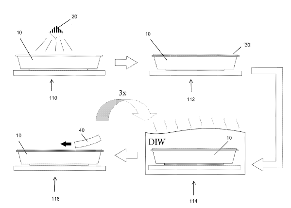
US9387521 — METHOD OF WET CLEANING ALUMINUM CHAMBER PARTS — Lam Research Corporation (USA) — A method of wet cleaning an aluminum part having bare aluminum surfaces and anodized aluminum surfaces. The method includes CO2 dry ice blasting the surfaces of the aluminum part at approximately 35 to approximately 45 psi, masking the aluminum part to conceal the bare aluminum surfaces, soaking the dry ice blasted and masked aluminum part in deionized water at or above approximately 60°C, scrubbing the aluminum part with an abrasive pad and deionized water after completion of the soaking in deionized water, and repeating the soaking and scrubbing in the recited order at least three additional times.
US9378897 — ELECTRODE MATERIAL FOR ALUMINUM ELECTROLYTIC CAPACITOR, AND PROCESS FOR PRODUCING SAME — Toyo Aluminium Kabushiki Kaisha (Japan) — The present invention provides an electrode material for an aluminum electrolytic capacitor, which does not require any etching treatment and which has improved bending strength. Specifically, the present invention provides an electrode material for an aluminum electrolytic capacitor, which comprises, as constituent elements, an anodized sintered body of a powder of at least one member selected from the group consisting of aluminum and aluminum alloys and an aluminum foil substrate that supports the sintered body thereon, which is characterized in that (1) the powder has an average particle size D50 of 0.5 to 100 µm, (2) the sintered body is formed on one surface or both surfaces of the aluminum foil substrate and has a total thickness of 20 to 1,000 µm, and (3) the aluminum foil substrate has a thickness of 10 to 200 µm and an Si content of 10 to 3,000 ppm.

US9373731 — DIELECTRIC STRUCTURES IN SOLAR CELLS — Newsouth Innovations PTY Limited (Australia) — The present invention relates generally to the field of device fabrication and to the formation of a structure that assists light trapping in solar cells. A dielectric, structure and a method of forming a dielectric structure for a rear surface of a silicon solar cell are provided. The method comprises forming a first dielectric layer over the rear surface of the silicon solar cell, and then depositing a layer of metal such as aluminum over the first dielectric layer. The metal layer is then anodized to form a porous layer and a material layer is deposited over a surface of the porous layer such that the material deposits on the surface of the porous layer without contacting the silicon surface.
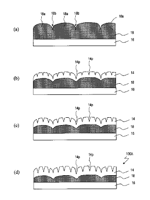
US9366785 — MOLD, METHOD FOR MANUFACTURING A MOLD, AND ANTIREFLECTIVE FILM — Sharp Kabushiki Kaisha (Japan) — Display devices for use in TVs, cell phones, optical elements, etc., usually adopt an antireflection technique in order to reduce the surface reflection and increase the amount of light transmitted therethrough. The present invention relates to a moth-eye mold with an antireflective structure, a method of fabricating a mold, and an antireflection film. In this specification, the “mold” includes molds that are for use in various processing methods (stamping and casting) and is sometimes referred to as a stamper. A moth-eye mold fabrication method includes: (a) providing an aluminum film deposited on a base, the aluminum film having a thickness of not less than 0.5 µm and not more than 5 µm, a surface of the aluminum film having a plurality of crystal grains whose average crystal grain diameter is not less than 200 nm and not more than 5 µm; (b) after step (a), anodizing the surface of the aluminum film to form a porous alumina layer which has a plurality of minute recessed portions; and (c) after step (b), bringing the porous alumina layer into contact with an etching solution, thereby enlarging the plurality of minute recessed portions of the porous alumina layer. A method of readily fabricating a mold is produced that is for manufacture of an antireflection film in which a moth-eye structure is superimposed over an antiglare structure.
US9353431 — HIGH-STRENGTH ALUMINUM ALLOY MATERIAL AND PROCESS FOR PRODUCING THE SAME — UACJ Corporation (Japan) — The present invention relates to a high-strength aluminum alloy material that can be used at portions of, e.g., transport machines, sporting goods, machine components, etc., where both strength characteristics and appearance characteristics are considered to be important. A high-strength aluminum material having a chemical composition which includes Zn: more than 7.2% (mass %, the same applies hereafter) and 8.7% or less, Mg: 1.3% or more and 2.1% or less, Cu: less than 0.50%, Fe: 0.30% or less, Si: 0.30% or less, Mn: less than 0.05%, Cr: 0.20% or less; Zr: less than 0.05%, Ti: 0.001% or more and 0.05% or less, the balance being Al and unavoidable impurities, is provided. It has a proof stress of 350 MPa or more, and a metallographic structure formed of a recrystallized structure. The recrystallized structure is comprised of crystal grains having an average particle diameter of 500 µm or less, and a crystal grain length in a direction parallel to a hot working direction is 0.5 to 4 times as long as a crystal grain length in a direction perpendicular to the hot working direction. After artificial aging and anodizing, the alloy product has excellent surface quality.
US9347146 — METHOD AND APPARATUS FOR FORMING A LAYERED METAL STRUCTURE WITH AN ANODIZED SURFACE — Apple Inc. (USA) — Methods and apparatus for forming a multi-layered metal structure that includes an anodized surface are disclosed. According to one aspect, a housing arrangement can include a stainless steel layer and at least a first layer. The first layer can have a first bonding surface and a first exterior surface. The first bonding surface can be substantially bonded in direct contact with the stainless steel layer, and the first exterior surface can be an exterior of the housing arrangement. The first exterior surface is an anodized surface. In one embodiment, the first layer can be formed from an anodizable material such as aluminum, titanium, niobium, or tantalum.

US9334577 — MULTIFUNCTIONAL COATING OF ALUMINUM PIECES — Airbus Operations GmbH (Germany) — the object of the present invention is to provide a method for applying a multifunctional coating to the surface of a workpiece consisting of aluminum or an aluminum alloy and a correspondingly coated workpiece which meets all three requirements: corrosion resistance, suitability for painting and suitability as a substrate for adhesive bonds, within a technical process chain. The invention is characterized by the production of an oxide film on workpieces made of aluminum or aluminum alloys. After being conventionally cleaned in grease removing and alkaline pickling baths, the aluminum components are subsequently introduced, for example into a Ce (IV)-containing picking bath and for further treatment are anodized such that the oxide layer which was produced in the cerium-containing pickling bath is not completely destroyed again. The parameters of the individual layer superstructures can be adjusted depending on the purpose of use–corrosion resistance or surface to be painted or adhesively bonded. The invention further relates to a workpiece, which may be produced by such a method.
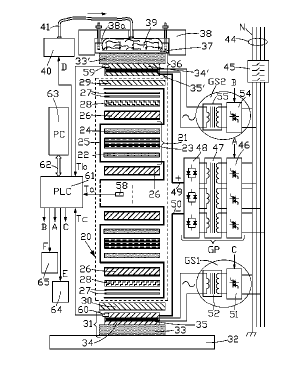
US9326390 — MANUFACTURING OF STACKS OF MULTILAYER PLASTIC LAMINATES FOR PRINTED CIRCUITS — Cedal Equipment SRL (Italy) — In manufacturing multilayer plastic laminates for printed circuits, a press with two surfaces exerts pressure under vacuum on a stack of laminates, the packs, alternated with separator plates made of anodized aluminum. The packs include prepreg layers. The metalizing present on the two sides of each pack are portions of a copper strip repeatedly folded 180.degree. around each pack and each separator plate. A strong current circulates in the copper strip which heats the strip with resistive behavior: the heat causes the close fixing of the various layers. An auxiliary heater is applied to each surface of the press by element of an interposed insulating plate. This includes an aluminum plate with equidistant longitudinal holes containing the same number of armored candle-like resistors, connected in parallel. A main power supply provides direct current to the copper strip, two secondary power supplies provide alternating current to the two auxiliary heaters.
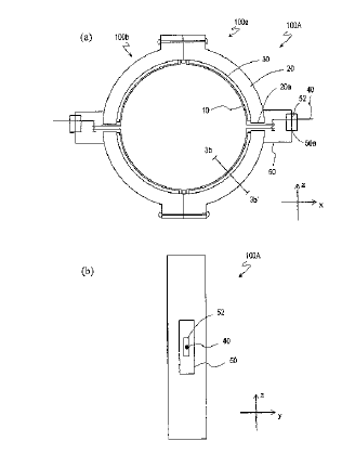
US9315916 — ELECTRODE STRUCTURE, SUBSTRATE HOLDER, AND METHOD FOR FORMING ANODIC OXIDATION LAYER — Sharp Kabushiki Kaisha (Japan) — An electrode structure of the present invention for anodizing a surface of an aluminum base includes: an aluminum electrode which is to be in contact with a surface of an aluminum base; a fixing member for fixing the aluminum electrode on the surface of the aluminum base; an elastic member provided between the fixing member and the aluminum base; a lead wire which is electrically connected to the aluminum electrode at least under a certain condition; and a cover member which is tightly closed with the lead wire penetrating through an opening.
US9310679 — MAKING LITHOGRAPHIC PRINTING PLATES — Eastman Kodak Company (USA) — This invention relates to imaging and processing positive-working lithographic printing plate precursors that have a unique acid dye in the layer adjacent to the substrate, using infrared radiation to provide lithographic printing plates. A thermally-sensitive, positive-working lithographic printing plate precursor can be used to prepare lithographic printing plates using high pH, silicate-free processing solutions. The precursor has a grained and anodized aluminum-containing substrate including a poly(vinyl phosphonic acid) interlayer. A first ink receptive layer, and optionally a second ink receptive layer, is disposed directly on the poly(vinyl phosphonic acid) interlayer. This first ink receptive layer comprises an aromatic acid dye that comprises at least two aromatic groups in an amount of least 0.5 weight %. In addition, the precursor comprises an infrared radiation absorber in one of the layers.
US9300036 — RADIO-FREQUENCY TRANSPARENT WINDOW — Apple Inc. (USA) — A patch for a device in an electronic housing including an aluminum layer having a threshold thickness, a non-conductive layer on a first side of the aluminum layer, and a radio-frequency (RF) transparent layer on a second side of the aluminum layer is provided. A method for manufacturing an antenna window including a patch as above is also provided, the method including determining a thickness of the aluminum layer adjacent to an anodized aluminum layer. A method for manufacturing an antenna window including coating an aluminum layer having a threshold thickness on a radio-frequency (RF) transparent layer to form an RF transparent laminate is also provided. A method for manufacturing an antenna window including removing a thickness of aluminum is also provided. A method for manufacturing an antenna window including disposing a mask on an aluminum substrate and anodizing the aluminum substrate to a selected thickness is also provided.
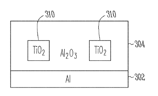
US9275801 — SYSTEMS AND METHODS FOR ENHANCED DIELECTRIC PROPERTIES FOR ELECTROLYTIC CAPACITORS — Cardiac Pacemakers, Inc. (USA) — This disclosure relates to apparatus for enhanced dielectric properties for electrolytic capacitors to store energy in an implantable medical device. A capacitor according to one embodiment includes an anode, a cathode, and a dielectric separating the anode and the cathode. The dielectric comprises aluminum oxide doped with a metal oxide having a dielectric constant greater than aluminum oxide, in various embodiments. One aspect of the present subject matter includes a method for manufacturing a capacitor adapted to be disposed in an implantable device housing. An embodiment of the method includes providing a dielectric comprising aluminum oxide and doping the aluminum oxide with an oxide having a dielectric constant greater than aluminum oxide. Doping the aluminum oxide includes using sol-gel based chemistry, electrodeposition or atomic layer deposition (ALD) in various embodiments.
US9265169 — HOUSING AND ELECTRONIC DEVICE USING THE HOUSING — Shenzhen Futaihong Precision Industry Co., Ltd. (China) and FIH (Hong Kong) Limited (Hong Kong) — A housing includes a substrate made of aluminum or aluminum alloy, an anodic oxide film disposed on the substrate, and an abrasion resisting layer disposed on the anodic oxide film. The abrasion resisting layer is an alkylate silicon dioxide layer containing nano aluminum oxide powder. An electronic device using the housing is also described. The abrasion resisting layer may be formed by spraying a silane coupling agent water solution on the anodic oxide film. The silane coupling agent contains Si-OH groups which can perform a condensation reaction with the -OH groups at the surface of the anodic oxide film to form Si-O-Si groups, thereby the abrasion resisting layer is firmly attached on the anodic oxide film, such that the abrasion resistance of the abrasion resisting layer and/or the housing is improved. Furthermore, since the alkylate silicon dioxide layer has a high hardness, the abrasion resistance of the abrasion resisting layer and/or the housing is further enhanced.

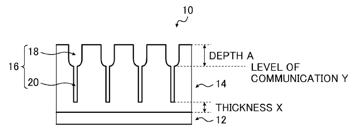
US9259954 — SUPPORT FOR LITHOGRAPHIC PRINTING PLATE AND MANUFACTURING METHOD THEREFOR, AS WELL AS ORIGINAL LITHOGRAPHIC PRINTING PLATE — FUJIFILM Corporation (Japan) — A lithographic printing plate support of the invention includes an aluminum plate and an anodized aluminum film which has micropores extending from a surface of the anodized film opposite from the aluminum plate in a depth direction of the anodized film; the micropores each have a large-diameter portion extending from the anodized film surface to an average depth (depth A) of 75 to 120 nm and a small-diameter portion which communicates with the bottom of the large-diameter portion; the average diameter of the large-diameter portion at the anodized film surface is at least 10 nm but less than 30 nm; a ratio of the depth A to the average diameter (depth A/average diameter) of the large-diameter portion is more than 4.0 but up to 12.0; and an average diameter of the small-diameter portion at the communication level is more than 0 but less than 10 nm.
US9229325 — METHOD FOR MAKING LITHOGRAPHIC PRINTING PLATES — Eastman Kodak Company (USA) — Lithographic printing plate are formed by imagewise exposing a positive-working lithographic printing plate precursor with infrared radiation to form an imaged precursor comprising exposed regions and non-exposed regions, and processing the imaged precursor to remove the exposed regions using a processing solution having a pH of 12 or more, that contains a metal cation M2+ selected from barium, calcium, strontium, and zinc cations, and is substantially silicate-free. The positive-working lithographic printing plate precursor comprises a grained and anodized aluminum-containing substrate, a first ink receptive layer comprising at least one water-insoluble, alkali solution-soluble or -dispersible first resin, a second ink receptive layer disposed over the first receptive layer, and an infrared radiation absorber in an amount of at least 0.5 weight %, in either or both of the first ink receptive layer and the second ink receptive layer.
US9209513 — ANTENNA WINDOW AND ANTENNA PATTERN FOR ELECTRONIC DEVICES AND METHODS OF MANUFACTURING THE SAME — Apple Inc. (USA) — A housing for an electronic device, including an aluminum layer enclosing a volume that includes a radio-frequency (RF) antenna is provided. The housing includes a window aligned with the RF antenna; the window including a non-conductive material filling a cavity in the aluminum layer; and a thin anodized aluminum oxide layer (<50 µm) adjacent to the aluminum layer and to the non-conductive material; wherein the non-conductive material and the thin aluminum oxide layer form an RF-transparent path through the window. A housing for an electronic device including an integrated RF-antenna is also provided. A method of manufacturing a housing for an electronic device as described above is provided.
US9207537 — LITHOGRAPHIC PRINTING ORIGINAL PLATE — FUJIFILM Corporation (Japan) — A surface of an aluminum alloy plate is subjected to a surface treatment process including surface roughening treatment and anodizing treatment to obtain a support, a photosensitive material is then applied to the support and dried to obtain a so-called PS plate, the PS plate is then subjected to a plate-making process including image exposure, development and gum coating, and the resulting plate is generally used as an offset printing plate or lithographic printing plate. A PS aluminum plate having a long press life and excellent resistance to scum and corrosive micro-stains and capable of on-press development is provided. The PS plate includes a photosensitive layer containing (A) a sensitizing dye, (B) a polymerization initiator, (C) a polymerizable compound, and (D) a binder polymer; and a protective layer which are formed on a support in this order. The support is prepared from an aluminum alloy plate containing intermetallic compound particles with a circle equivalent diameter of 0.2 µm or more at a surface density of 35,000 pcs/mm2 or more and aluminum carbide particles with a maximum length of 1 µm or more in an amount of up to 30,000 pcs/g.
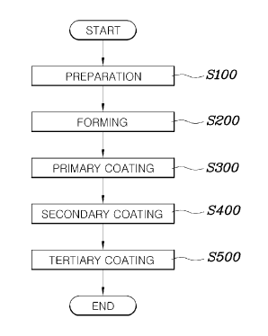
US9200664 — WHEEL NUT AND METHOD OF MANUFACTURING WHEEL NUT — Hyundai Motor Company and Kia Motors Corporation (Korea) — Disclosed herein is a method of manufacturing a wheel nut. The method includes annealing an aluminum (Al) alloy material and preheating the annealed Al alloy material. The Al alloy material is also forged to form a wheel nut. Furthermore, the method includes performing an anodizing treatment to form a primary coating on the wheel nut and performing a vacuum deposition to form a secondary coating on the wheel nut. In addition, the method includes performing a surface treatment using powder paint to form a tertiary coating on the wheel nut.
US9193096 — DIE, DIE PRODUCTION METHOD, AND PRODUCTION OF ANTIREFLECTION FILM — Sharp Kabushiki Kaisha (Japan) — The present invention relates to a mold, a mold manufacturing method, and an antireflection film production method. In this specification, the “mold” includes molds that are for use in various processing methods (stamping and casting) and is sometimes referred to as a stamper. One of the objects of the present invention is to provide a method for readily manufacturing a seamless mold in the form of a roll which has a porous alumina layer over its surface. The mold manufacturing method of the present invention is a method for manufacturing a mold which has a porous alumina layer over its surface, including the steps of: providing a hollow cylindrical support; forming an insulating layer on an outer perimeter surface of the hollow cylindrical support; depositing aluminum on the insulating layer to form an aluminum film; and anodizing a surface of the aluminum film to form a porous alumina layer which has a plurality of minute recessed portions.
US9188704 — OPTICAL FILM AND METHOD FOR MANUFACTURING THE SAME — Hon Hai Precision Industry Co., Ltd. (Taiwan) — The present invention relates to an optical film and a method of manufacturing an optical film which has anti-reflective and self-cleaning properties. A method of manufacturing an optical film includes: providing a template; coating an aluminum film on one surface of the template; anodizing the aluminum film and generating a plurality of regular microstructures on the aluminum film; providing a substrate; transferring the microstructures of the template to the substrate to form a plurality of microstructures on the substrate; and modifying the surfaces of the microstructures of the substrate to obtain a layer containing hydrophobic functional groups on the surfaces of the microstructures of the substrate.
US9142359 — ELECTRODE MATERIAL FOR ALUMINUM ELECTROLYTIC CAPACITOR AND PROCESS FOR PRODUCING THE ELECTRODE MATERIAL — Toyo Aluminium Kabushiki Kaisha (Japan) — The present invention provides an electrode material for use in an aluminum electrolytic capacitor that does not necessitate an etching treatment. Specifically, the present invention provides an electrode material for use in an aluminum electrolytic capacitor, the electrode material comprising an anodized sintered body of at least one of aluminum and an aluminum alloy. The present invention can provide an electrode material comprising a sintered body, which is different from a conventional electrode material (rolled foil) having etching pits. Such a sintered body particularly has a unique structure in which particles (particularly, aluminum or aluminum alloy powder particles) are sintered while a space is maintained between each particle. Because of this structure, an electrostatic capacity equivalent to or greater than that of a conventional etched foil can be obtained. Therefore, the present invention can be substituted particularly for an etched foil having thick etching pits for use in medium- to high-voltage capacitors.
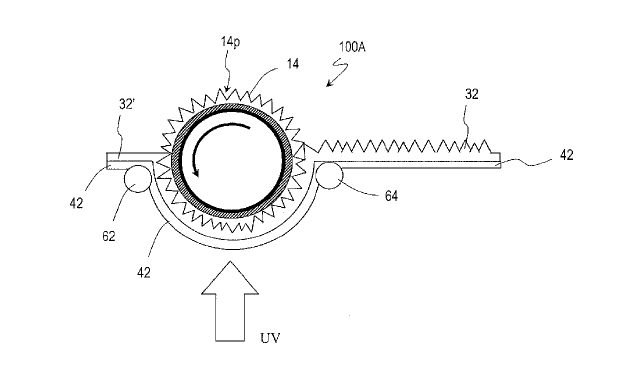
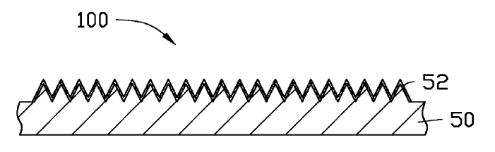
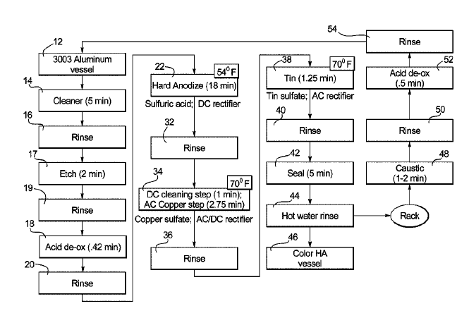
US9139926 — PROCESS FOR MAKING HEAT STABLE COLOR ANODIZED ALUMINUM AND ARTICLES FORMED THEREBY — Calphalon Corporation (USA) — The present invention is generally directed to a process whereby an aluminum article can be hard anodized and yet achieve a colored surface. The colored anodized surface of the aluminum article produced by the disclosed process is also capable of withstanding repeated exposure to temperatures well above 375°F. Such temperatures are achieved every day by consumers under normal cooking conditions that traditional cookware must be capable of withstanding. A process of hard anodizing or Type III anodizing an aluminum article creates a heat stable, hard anodized, color surface on the exterior of the article. The process includes anodizing the aluminum article to achieve a hard anodized base layer on a surface of the article. A copper layer is deposited after the exterior is hard anodized. A tin layer is deposited after the step of depositing the copper layer.
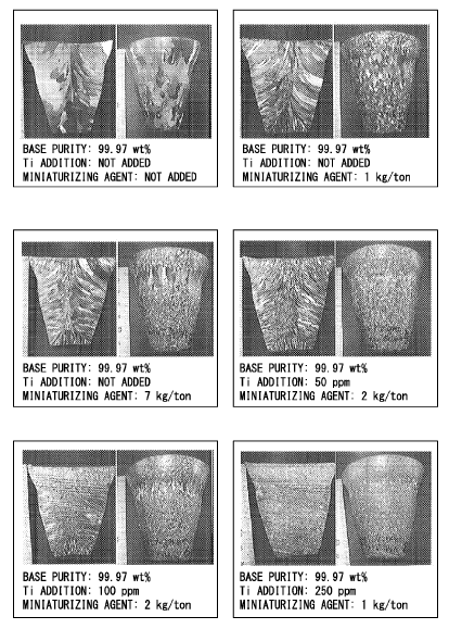
US9138936 — STAMPER, ARTICLE AND METHOD FOR MANUFACTURING THE SAME STAMPER, ARTICLE AND METHOD FOR MANUFACTURING THE SAME — Nippon Light Metal Company Ltd. and Mitsubishi Rayon Co., Ltd. (Japan) — In a case in which the surface of aluminum is anodized so as to produce a stamper, and the surface is transferred so as to manufacture an article, since the shape of the surface of the stamper is mirrored at the surface of a transfer target as it is, the regularity or shape of the surface of the stamper is important in terms of the antireflection function from the liquid crystal surface of a television, a mobile phone or the like. The invention relates to a stamper in which an oxide film having a fine concave-convex structure made up of a plurality of fine pores having an aspect ratio represented by the depth of the fine pores/the average interval between the fine pores of 1 to 4 is formed on the surface of an aluminum base material which is made of aluminum having a content of Ti of 150 ppm to 500 ppm, a content of B or C of 1 ppm to 50 ppm and a purity of 99.9% or more. According to the invention, it is possible to provide a low-cost stamper in which the emergence of a pattern derived from the traces of crystal grains on the surface of the oxide film is suppressed, an article having a favorable appearance, which is manufactured using the above stamper, and a method for manufacturing the above.
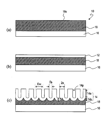
US9133558 — METHOD FOR PRODUCING ANODIZED FILM — Sharp Kabushiki Kaisha (Japan) — An antireflection technique is forming over a substrate surface a very small uneven pattern in which the interval of recessed portions or raised portions is not more than the wavelength of visible light, a so-called “moth-eye” structure that performs an antireflection function is not less than 10 nm and less than 500 nm. As the method of forming a moth-eye structure, using an anodized porous alumina layer which is obtained by means of anodization of aluminum, according to an embodiment of the present invention includes the steps of: (a) providing a multilayer structure that includes a base, a sacrificial layer which is provided on the base and which contains aluminum, and an aluminum layer which is provided on a surface of the sacrificial layer; (b) partially anodizing the aluminum layer to form a porous alumina layer which has a plurality of minute recessed portions; and (c) after step (b), separating the porous alumina layer from the multilayer structure. According to an embodiment of the present invention, a self-supporting anodized film which includes a porous alumina layer can be manufactured more conveniently as compared with the conventional methods.

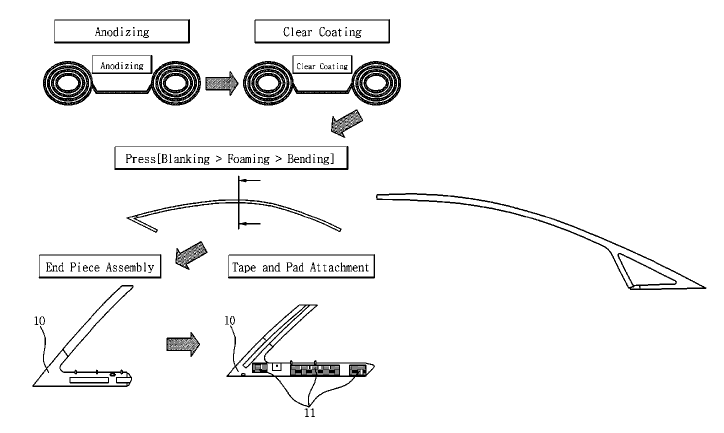
US9132474 — METHOD FOR MANUFACTURING LIGHT-REFLECTION ALUMINUM DOOR FRAME MOLDING — Hyundai Motor Company Korea) — Disclosed is a method for manufacturing a light-reflection aluminum door frame molding which comprises a multi-coating-applied aluminum material to thereby improve corrosion resistance and reduce costs. A method for manufacturing a light-reflection aluminum door frame molding includes cutting a metallic plate into a predetermined size, performing anodizing on the metallic plate to form an oxidized film on a surface thereof, performing opaque clear coating and transparent coating on the metallic plate to implement light reflection, and performing press molding on the metallic plate to provide the metallic plate in the shape of a door frame molding.
US9108351 — METHOD FOR FORMING ANODIZED LAYER, METHOD FOR PRODUCING MOLD AND METHOD FOR PRODUCING ANTIREFLECTIVE FILM — Sharp Kabushiki Kaisha (Japan) — Display devices for use in TVs, cell phones, etc., and optical elements, such as camera lenses, etc., usually adopt an antireflection technique in order to reduce the surface reflection and increase the amount of light transmitted therethrough. The method of forming an antireflective “moth-eye” structure, using an anodized porous alumina layer of an embodiment of the present invention includes the step a of providing an aluminum film which is formed on a first principal surface of a support and the step b of anodizing a surface of the aluminum film to form a porous alumina layer which has a plurality of minute recessed portions. In the step a, a second principal surface of the support which is opposite to the first principal surface is provided with a low heat conduction member that has a predetermined pattern. According to an embodiment of the present invention, a porous alumina layer can be formed which includes regions of different minute structures in the predetermined pattern.
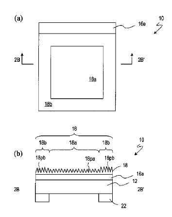
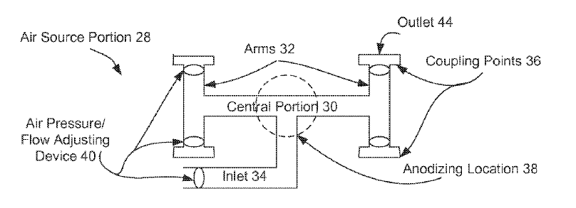
US9096944 — AIR DISTRIBUTION SYSTEM FOR ANODIZING TANK — Dell Products L.P. (USA) — Information handling system metal housing portions, such as aluminum portions, are anodized in an electrolyte bath agitated by a balanced air deliver system that reduces dead zones for improved chemical distribution and consistent temperatures at the metal housing portion. Equal-sized air distribution portions selectively couple to an air distribution portion to provide an air distribution system with balanced air delivery and which anodizes metal in a consistent bath that provides improved cosmetics of the metal end product, such as an information handling system.